Friday 29 March 2013

Monday 25 March 2013


Sunday 24 March 2013


Saturday 23 March 2013


Friday 22 March 2013
PROPERTIES OF RL IMPEDANCE OR RC ADMITTANCE
1) Poles and zeros are alternating
2) Poles and zeros are simple and lie on the negative real
axis of the s-plane.
3)The critical frequency nearest to origin is a zero
4) The critical frequency farthest from origin is a pole
5)The residues of Y(s) at its poles are all negative and
real
6) The slope of YRC(σ) is positive and the slope of YRC(-σ)
is negative
7) YRC(∞)≥YRC(0)
Methods
for realising a RC IMPEDANCE OR RL ADMITTANCE function
1) Foster
form 1
2)
Foster form 2
3) Cauer
form 1
4)
Cauer form 2
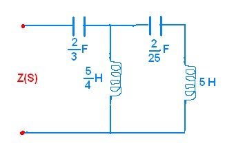
FOSTER FORM 1
It is used to realize impedance function.
FOSTER FORM 1
It is used to realize impedance function.


Friday 22 March 2013 0
Thursday 21 March 2013
PROPERTIES OF RC IMPEDANCE OR RL ADMITTANCE
1)Poles and zeros are alternating
2) Poles and zeros are simple and lie on the negative real
axis of the s-plane.
3)The critical frequency nearest to origin is a pole which
indicates a capacitor for RC impedance
4) The critical frequency farthest from origin is a zero which indicates a capacitor for
RC impedance
5)The residues of Z(s) at its poles are all positive and
real
6) The slope of ZRC(σ) is negative and the slope of ZRC(-σ)
is positive
7) ZRC(0)
≥ZRC(∞)
Methods
for realising a RC IMPEDANCE OR RL ADMITTANCE function
1) Foster
form 1
2)
Foster form 2
3) Cauer
form 1
4)
Cauer form 2


Thursday 21 March 2013 0
Tuesday 19 March 2013

Switch
connected to +VM
Once
VM is connected, the capacitor starts charging linearly then the
output at the integrator decreases linearly. This linearly decreasing ramp is
fed to inverting terminal of the zero crossing detector. Since the input at non
inverting terminal is greater than inverting terminal, it produces a positive
going pulse. This positive going pulse makes the gating circuit to start. Now pulses
produced by the clock generator passess through gating circuit and counter
count the number of pulses.

t
VC
= 1/C ∫ I dt
-∞
t1
= 1/C ∫ VM / R dt
0
=
VM
/ RC ( t1 – 0 )
= VMt1/RC
=
VMT1/RC (t1 =T1)
V0
= -VC
V0
= - ( VMT1/RC )
Graphs
of VC and V0
Tuesday 19 March 2013 0
Sunday 17 March 2013
TO READ THE SPECIFIC TOPIC CLICK ON THE LINK GIVEN BY THE SIDE OF EACH TOPIC
INTRODUCTION TO DVMs
DIGITAL READOUTS OF DVMs
TYPES OF DVMs
RAMP TYPE
DUAL SLOPE INTEGRATING TYPE

OPERATION
This DVM measures unknown voltage VM by measuring
the time taken by a linearly falling ramp voltage to fall from unknown voltage
level to zero volts
Ramp generator produces a decreasing OR increasing ramp
Input comparator generates starting pulse to open gate
circuit
Output generator produces stop pulse to close gate circuit
Clock generator produces pulses
Decade counter calculates number of pulses that pass through
it
AT INPUT COMPARATOR
An unknown voltage VM is given to the input of
non inverting terminal. When the input at inverting terminal of op-amp is less
than VM out at the input comparator is positive otherwise it is negative.
When VR decreases below VM it produces a positive going pulse,
this pulse makes the gating circuit to start and the pulse produced by the
clock generator passes through the gating circuit. These pulses are counted by
decade counter

AT GROUND COMPARATOR
Ground comparator or zero level detector .so when the VR crosses zero and moves to negative values, the input at inverting terminal is greater than non inverting terminal. So output of this comparator produces a negative going pulse which makes the gating circuit to stop. Therefore the reading displayed on the display is the unknown voltage.
Ground comparator or zero level detector .so when the VR crosses zero and moves to negative values, the input at inverting terminal is greater than non inverting terminal. So output of this comparator produces a negative going pulse which makes the gating circuit to stop. Therefore the reading displayed on the display is the unknown voltage.
VOLTAGE TO TIME CONVERSION

VR ------------TR
VM ----------TM
VM = ( VR / TR )*TM
Time period measurement
Let TCLK be time
period of clock generator. Let ‘n ‘ be the number of clock pulses between T1
and T2
T2 – T1 = TM = n* TCLK
Substitute the value of TM in VM we get
VM = ( VR / TR )* n *TCLK
FEATURES OF RAMP TYPE DVM
1)CONVERSION TIME
TCONV = TM = nTCLK
Where n is proportional to | VM | because the number of pulses depends upon VM
Where n is proportional to | VM | because the number of pulses depends upon VM
2) NOISE REJECTION
If either AC signal or noise is superimposed on unknown DC
voltage then error is introduced in voltage measurement. So noise affect is more.
Therefore noise rejection is poor. Since stability of DVM depends on noise condition.
Its stability is poor.
3) ACCURACY
Value Internal components of ramp generator changes due to
aging then linearity of ramp changes then VM also changes as shown
in the figure and accuracy of measurement is affected.

Saturday 16 March 2013

The sinusoidal waveform of figure 1 with its additional notation will now be used as a model in defining a few basic terms. These terms, however, can be applied to any alternating waveform. It is important to remember as you proceed through the various definitions that the vertical scaling is in volts or amperes and the horizontal scaling is always in units of time.
Waveform
The path traced by
a quantity, such as the voltage in figure 1, plotted as a function of some
variable such as time (as above), position, degrees, radians, temperature, and
so on.
Instantaneous value
The
magnitude of a waveform at any instant of time; denoted by lowercase letters
(e1, e2).
Saturday 16 March 2013 0
In 3 / 4 digit numerator
indicates maximum value and denominator indicates number of digits
Number of digits
|
Maximum value
|
|
9/10
|
0,1,2,3………9
|
9
|
1/2
|
0,1
|
1
|
3/4
|
0,1,2,3
|
3
|
Note
A full digit has decimal
point but ½ , ¾ … doesn’t have decimal point
Example

( 0 – 1 )V 3 digit DVM
SOLUTION
Subscribe to:
Posts (Atom)


