Wednesday 27 February 2013
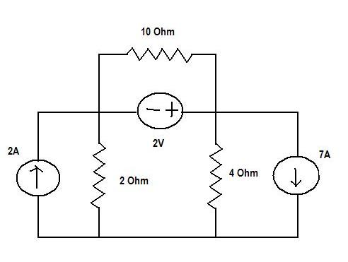
If the network contains more than one voltage or current source, superposition allows for a solution to be found by considering each voltage or current source separately and then adding the results. To consider each source separately, all other voltage sources are open circuited and all other current sources are short circuited.

Wednesday 27 February 2013 4
Sunday 24 February 2013

Sunday 24 February 2013 8
Saturday 23 February 2013
Saturday 23 February 2013 1
Sunday 17 February 2013

Sunday 17 February 2013 0
Friday 15 February 2013
NOTE :Click on the topic,wait for 5 sec and press skip ad
1 ) KCL AND KVL
2) OHM'S LAW
3) RESISTOR
4) INDUCTOR
5) CAPACITOR
6) NODAL ANALYSIS
7) SUPER NODE ANALYSIS
8) MESH ANALYSIS
9) SUPER MESH ANALYSIS
10)TECHNIQUES IN CIRCUIT SOLVING
SUPERPOSITION THEOREM
THEVENIN AND NORTON'S THEOREM
MODELS IN THEVENIN AND NORTON'S THEOREM
TYPE -1
TYPE -2
TYPE -3
MAXIMUM POWER TRANSFER
RECIPROCITY THEOREM
MILLMAN’S THEOREM
TRANSIENTS AND BEHAVIOR OF STORAGE ELEMENTS
BEHAVIOR OF CAPACITOR & INDUCTOR AT t= 0- AND t=0+
SOURCE FREE CIRCUITS
SOURCE FREE RL CIRCUIT
SOURCE FREE RC CIRCUIT
NATURAL RESPONSE OF RLC CIRCUIT
PROBLEM 1
PROBLEM 2
PROBLEM 3
COUPLED CIRCUITS
PROBLEM 1
PROBLEM 2
Friday 15 February 2013 0
41. Define input offset voltage?
It is defined as the voltage that must be applied between the input terminals of an op-amp to nullify the output.
42. Define input offset current?
It is defined as the algebraic difference between the current entering the inverting and non-inverting terminal of an op-amp.
43. Define input bias current?
It is defined as the average of the currents entering into the input terminals of an op-amp.
44. What are the two compensating techniques used in frequency compensation?
Two types of compensating techniques are used, they are,
a. External compensation
b. Internal compensation
45. What is compensated op-amp?
Op-amp, which uses a capacitor internally for compensation, is called a compensated op-amp. This op-amp has a high gain stability and low bandwidth.
46. What are the methods used in external compensation technique?
a. Dominant-pole compensation
b. Pole-zero compensation
47. Define slew rate?
Slew rate can be defined as the maximum rate of change of output voltage of op-amp with respect to time.
48. How can the slew rate be made faster?
The slew rate can be made faster by having a high charging current or a small capacitance value.
49. What are the methods to improve slew rate?
a. The slew rate can be improved with higher closed-loop gain and dc supply voltage. But
Thursday 14 February 2013
1.Define an Integrated circuit.
An integrated circuit(IC) is a miniature ,low cost electronic circuit consisting of active and passive components fabricated together on a single crystal of silicon.The active components are transistors and diodes and passive components are resistors and capacitors
.
2.What are the basic processes involved in fabricating ICs using planar technology?
1.Silicon wafer (substrate) preparation
2.Epitaxial growth
3.Oxidation
4.Photolithography
5.Diffusion
6.Ion implantation
7.Isolation technique
8.Metallization
9.Assembly processing & packaging
3.List out the steps used in the preparation of Si – wafers.
1.Crystal growth &doping
2.Ingot trimming & grinding
3.Ingot slicing
4.Wafer policing & etching
5.Wafer cleaning
4. Write the basic chemical reaction in the epitaxial growth process of pure silicon.
The basic chemical reaction in the epitaxial growth process of pure silicon is the hydrogen reduction of silicon tetrachloride.
1200oC
5. What are the two important properties of SiO2?
1.SiO2 is an extremely hard protective coatng & is unaffected by almost all reagents except by
Thursday 14 February 2013 0
21. What is an amplifier?
An amplifier is a device which produces a large electrical output of similar characteristics to that of the input parameters.
22. How are amplifiers classified according to the input?
1. Small – signal amplifier
2. Large – signal amplifier
23. How are amplifiers classified according to the transistor configuration?
1. Common emitter amplifier
2. Common base amplifier
3. Common collector amplifier
24. What is the different analysis available to analyze a transistor?
1. AC analysis
2. DC analysis
25. How can a DC equivalent circuit of an amplifier be obtained?
By open circuiting the capacitor.
26. How can a AC equivalent circuit of a amplifier be obtained?
By replacing dc supply by a ground and short- circuiting capacitors.
27. What is feed back?
It is the process of injecting some energy from the output and then returns it back to the input.
28. What are feed back amplifiers?
Amplifiers which uses feed back principle is called as feed back amplifiers.
29. What are the types of feed back?
1. Positive feedback
2. Negative feedback.
30. What is positive feedback?
If the feed back signal is applied in such a way that it is in phase with the input signal and thus increases it is said to be positive feedback.
31. What is negative feed back?
If the feed back signal is applied in such a way that it is out of phase with the input signal and thus decreases it is said to be positive feedback.
32. Which feedback decreases the gain of the amplifier?
Negative feed back
33. Which feedback increases the gain of the amplifier?
Positive feedback
34. What is the advantage of negative feed back?
1. increased stability
2. Increased bandwidth
3. Decreased noise
4. Less frequency distortion
35. What is the disadvantage of negative feed back?
Reduces amplifier gain.
36. Define sensitivity.
It is the ratio of percentage change in voltage gain with feedback to the percentage change in voltage gain without feed back.
37. Define Desensitivity.
It is the ratio of percentage change in voltage gain without feedback to the percentage change in voltage gain with feed back. the reciprocal of sensitivity.
38. What is an op-amp?
The operational amplifier is a multi-terminal device, which is quite complex internally. An operational amplifier is a direct coupled high gain amplifier usually consisting of one or more differential amplifiers and usually
followed by a level translator and an output stage. An operational amplifier is available as a single integrated circuit package. It is a versatile device that can be used to amplify dc as well as ac input signals and was originally designed for computing such mathematical functions.
39. What are the characteristics of ideal op-amp?
a. Open loop voltage gain, (AOL) = ’infinity
b. Input impedance (Ri) = ’’infinity
c. Output impedance (Ro) = 0
d. Bandwidth (BW) = ’’infinity
e. Zero offset Vo = 0, when V1 = V2 = 0
40. Define loading?
A large value of Rc cannot be used in a circuit since,a large value of resistance requires a large chip area.
For large Rc, quiescent drop across it increases and hence a large power supply is required.
These difficulties removed by using a current source. Hence, a current source can also be used as an active load for an amplifier to obtain a very large voltage gain
The net flow of electrons and holes in a semiconductor will generate currents.
The process by which these charged particles move is called transport.
There are the two basic transport mechanisms in a semiconductor crystal:
Drift the movement of charge due to electric fields, and
Diffusion the flow of charge due to density gradients.
The carrier transport phenomena are the foundation for finally determining the current-voltage characteristics of semiconductor devices.
We will implicitly assume that, though there will be a net flow of electrons and holes due to the transport processes, thermal equilibrium will not be substantially disturbed.
Carrier Drift
An electric field applied to a semiconductor will produce a force on electrons and holes so that they will experience a net acceleration and net movement, provided there are available energy states in the conduction and valence bands.
This net movement of charge due to an electric field is called drift.
The net drift of charge give, rise to a drift current.
However, charged particles in a semiconductor are involved in collisions with ionized impurity atoms and with thermally vibrating lattice atoms.
These collisions, or scattering events, alter the velocity characteristics of the particle.
As the hole accelerates in a crystal due to the electric fi eld, the velocity increases.
When the charged particle collides with an atom in the crystal, for example, the particle loses most or all of its energy.
The particle will again begin to accelerate and gain energy until it is again involved in a scattering process.
This continues over and over again.
Throughout this process the particle will gain an average drift velocity which, for low electric fields, is directly proportional to the electric field.
Carrier Diffusion
There is a second mechanism that can induce a current in a semiconductor.
We may consider a classic physics example in which a container, as shown in Figure , is divided into two parts by a membrane.
The left side contains gas molecules at a particular temperature and the right side is initially empty.
The gas molecules are in continual random thermal motion so that, when the membrane is broken, the gas molecules flow into the right side of the container.
Diffusion is the process whereby particles flow from a region of high concentration toward a region of low concentration.
If the gas molecules were electrically charged, the net flow of carriers would result in a diffusion current.
MOBILITY

 is the drift velocity (m/s)
 is the magnitude of the applied electric field (V/m)
 is the mobility (m2/(V.s))


Speed = distance / time


